Introduction
Operational Amplifier is internally a Differential Amplifier (its first stage) with other important features like High Input Impedance, Low Output Impedance etc. For more information on Op-Amp, read Operational Amplifier Basics. The Differential Pair or Differential Amplifier configuration is one of the most widely used building blocks in analog integrated-circuit design. It is the input stage of every Operational Amplifier. A Difference Amplifier or a Differential Amplifier amplifies the difference between the two input signals. An operational amplifier is a difference amplifier; it has an inverting input and a non-inverting input. But the open loop voltage gain of an operational amplifier is too high (ideally infinite) to be used without a feedback connection. So, a practical differential amplifier uses a negative feedback to control the voltage gain of the amplifier.
Differential Amplifier
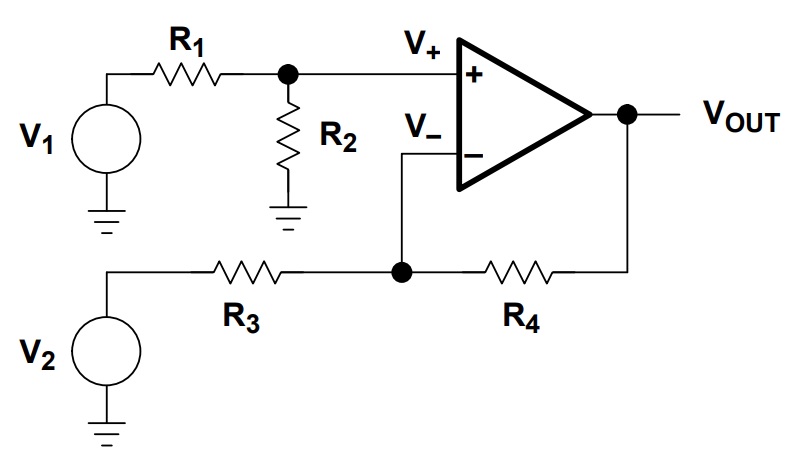
The following image shows a simple Differential Amplifier using an Op Amp. Here, V1 is the Non-Inverting Input Voltage, V2 is the Inverting Input Voltage and VOUT is the Output Voltage.
If you observe the above circuit of the difference amplifier, it is a combination of both the Inverting Amplifier and the Non-Inverting Amplifier. So, to calculate the output voltage of a Differential Amplifier, we will use both the Inverting and Non-Inverting outputs and add them together.
Calculating the Output Voltage
Let V+ be the voltage at the Non-Inverting terminal and V– be the voltage at the Inverting Terminal of the above Differential Amplifier Circuit. We can calculate the value of V+ using the Potential Divider Rule. Resistors R1 and R2 form a Voltage Divider Network with V1 as the Input Voltage and V+ as the output voltage and this V+ is applied at the non-inverting terminal. So, V+ = V1 (R2 / R1 + R2) If V+ is the input to the non-inverting terminal and G+ is the gain of the Non-Inverting Amplifier, then non-inverting output VOUT+ is given by: VOUT+ = V+ G+ From the above circuit, we can calculate the Non-Inverting Gain G+ as: G+ = (R3 + R4) / R3 = 1 + (R4 / R3) Using the values of V+ and G+ in the equation of VOUT+, we get VOUT+ = V1 (R2 / R1 + R2) (1 + (R4 / R3)) Coming to the Inverting Output VOUT–, we have to calculate it with respect to the inverting input V2 and the Inverting Gain G–. VOUT– = V2 G– From the above circuit, we can calculate the Inverting Gain G– as: G– = – R4 / R3 So, VOUT– is given by: VOUT– = V2 (– R4 / R3) We have both VOUT+ and VOUT– values. To get the final VOUT value, we have to add these values. VOUT = VOUT+ + VOUT– VOUT = V1 (R2 / R1 + R2) (1 + (R4 / R3)) – V2 (R4 / R3) This is the output voltage of a Differential Amplifier. The above equation looks complex. So, to reduce the complexity and simply the equation, let us take a special case where R3 = R1 and R4 = R2. If we apply these values in the above equation, we the output voltage as: VOUT = R2 / R1 (V1 – V2) = R4 / R3 (V1 – V2) Now, from this equation, it is clear that the differential voltage (V1 – V2) is multiplied by the gain R2 / R1. Hence, it is Differential Amplifier.
Alternative way to Calculate Output Voltage
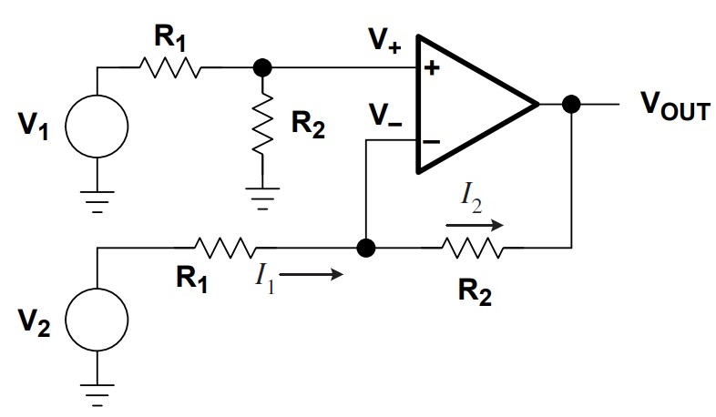
Let us now calculate the output voltage by determining the current at the Inverting Input of the Op Amp. Let us assume the following circuit for a Differential Amplifier. This circuit is similar to the previous one, except this a special case of R3 = R1 and R4 = R2 of the previous circuit.
First, we have to determine the voltage at the Non-Inverting terminal (V+). We already calculated this in the previous derivation using the voltage divider rule. The value is given by: V+ = V1 (R2 / R1 + R2) Now, from the basic understanding of the Operational Amplifier, we can say that no current flows in or out of the Op Amp input terminals. So, the current entering the Inverting Terminal I1 is same as the current leaving the terminal I2. I1 = I2 Using this rule as a reference, we can apply Kirchhoff’s Current Law at the Inverting Input Terminal and we get: (V2 – V–) / R1 = (V– – VOUT) / R2 Another important rule about Operational Amplifier is that it tries to keep the Input Terminals at same voltage. So, V+ = V–. Using this rule, we can replace V– in the above equation with the previously calculated V+ value. After replacing and performing some calculations, we arrive at: VOUT = R2 / R1 (V1 – V2) NOTE: In all the previous calculations, we took a special as R3 = R1 and R4 = R2. Actually, instead of this we have to consider the ratios i.e., R3 / R4 = R1 / R2 If this condition is used, then the resistances are said to be in a Balanced Bridge.
Important Parameters of Differential Amplifier
Let us now see some of the important parameters of a Difference Amplifier. They are:
Gain Common Mode Input Common Mode Rejection Ratio (CMRR)
Differential Amplifier Gain
The gain of a difference amplifier is the ratio of the output signal and the difference of the input signals applied. From the previous calculations, we have the output voltage VOUT as VOUT = R2 / R1 (V1 – V2) So, Differential Amplifier Gain AD is given by AD = VOUT / (V1 – V2) = R2 / R1
Common Mode Input
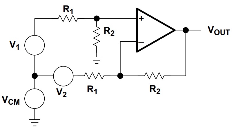
In all the previous calculations, we assumed the Balanced Bridge condition i.e., R3 / R4 = R1 / R2. To understand a unique characteristic of the Differential Amplifier or Difference Amplifier, we have to take a look at the Differential Mode Input and Common Mode Input Components. The Differential Mode Input VDM and Common Mode Input VCM are given by: VDM = V1 – V2 VCM = (V1 + V2) / 2 Rearranging the above two equations, we get V1 = VCM + VDM / 2 and V2 = VCM – VDM / 2 The following circuit shows the Common Mode Input Signals.
As the Difference Amplifier amplifies only the Difference Mode component, it ignores the Common Mode Component. If we tie the inputs together, the VDM becomes 0 and the VCM is a non-zero value. But a true Differential Amplifier will result in VOUT = 0, as it completely ignores the Common Mode portion of the input signal. Due to this, the Differential Amplifier is often used at the input stage of a system to strip the DC or the Common-Mode noise from the input. All these calculations are true if and only if the Resistances form the Balanced Bridge Condition. Since the output of a practical difference amplifier depends upon the ratio of the input resistances, if these resistor ratios are not exactly equal, the common mode voltage VCM will not be completely cancelled. Because it is practically impossible to match resistor ratios perfectly, there is likely to be some common mode voltage. With the common mode input voltage present, the output voltage of the differential amplifier is given as, VOUT = AD VDM + AC VCM Where VDM is the difference voltage V1 – V2 VCM is the common mode voltage (V1 + V2) / 2 AD and AC are Differential Mode and Common Mode Gains respectively.
Common Mode Rejection Ratio (CMRR)
The ability of a Differential Amplifier to reject common mode input signals is expressed in terms of Common Mode Rejection Ratio (CMRR). The Common Mode Rejection Ratio of a Differential Amplifier is mathematically given as the ratio of Differential Voltage gain (AD) of the Differential Amplifier to its Common Mode gain (AC). CMRR = AD / AC In terms of decibels (dB), the CMRR is expressed as CMRRdB = 20 log10 (| AD / AC |) For an ideal Difference Amplifier, the common mode voltage gain is zero. Hence, the CMRR is infinite.
Characteristics of a Differential Amplifier
High Differential Voltage Gain Low Common Mode Gain High Input Impedance Low Output Impedance High CMRR Large Bandwidth Low offset voltages and currents
Differential Amplifier as Comparator
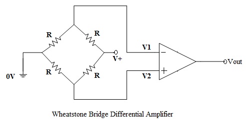
A Differential Amplifier circuit is a very useful Op Amp circuit, since it can be configured to either “add” or “subtract” the input voltages, by suitably adding more resistors in parallel with the input resistors. A Wheatstone Bridge Differential Amplifier circuit design is as shown in the following image. This circuit behaves like a Differential Voltage Comparator.
By connecting one input to a fixed voltage and the other to a thermistor (or a light-dependent resistor), the differential amplifier circuit detects high or low levels of temperature (or intensity of light) as the output voltage becomes a linear function of the changes in the active leg of the resistive bridge network. A Wheatstone Bridge Differential Amplifier can also be used to find the unknown resistance in the resistive bridge network, by comparing the input voltages across the resistors.
Light Activated Switch using Differential Amplifier
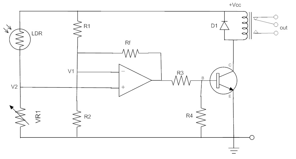
The circuit shown in the following image acts as a light-dependent switch, which turns the output relay either “ON” or “OFF” as the intensity of the light falling upon the light-dependent resistor (LDR) exceeds or falls below a pre-set value at the non-inverting input terminal V2.
The voltage V2 is determined by the variable resistor VR1. The resistors R1 and R2 act as a potential divider network. A fixed reference voltage is applied to the inverting input, through R1 and R2. The same circuit can be modified to detect variations in temperature, simply by replacing the LDR with a Thermistor. By interchanging the positions of LDR and VR1, the circuit can be made to detect dark or light (or heat or cold in case of a thermistor).
Differential Amplifier Example
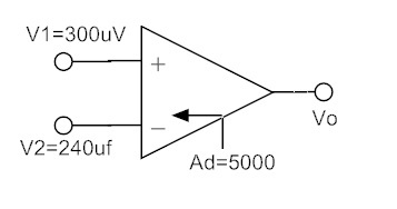
Determine the output voltage of a differential amplifier for the input voltages of 300 µV and 240 µV. The differential gain of the amplifier is 5000 and the value of CMRR is (i) 100 (ii) 105 The differential amplifier for the given data is represented as shown in the figure.
For CMRR = 100: CMRR = AD / AC 100 = 5000 / AC So, AC = 50 Difference Mode Voltage VDM VDM = V1 – V2 = 300 µV – 240 µV = 60 µV Common Mode Voltage VCM VCM = (V1 + V2) / 2 = 540 µV / 2 = 270 µV Output Voltage VOUT VOUT = AD VDM + AC VCM = 5000 x 60 µV + 50 x 270 µV VOUT = 313500 µV = 313.500 mV For CMRR = 105: AC = AD / CMRR = 5000 / 105 = 0.05 VOUT = AD VDM + AC VCM = 5000 x 60 µV + 0.05 x 270 µV VOUT = 300013.5 µV = 300.0135 mV NOTE: For ideal Difference Amplifier or Differential Amplifier, AC is 0. So, the output is only AD VDM, which results in VOUT = 5000 x 60 µV = 300 mV.
Differential Amplifier Summary
A Differential Amplifier, also known as Difference Amplifier, is a very useful op-amp configuration that amplifies the difference between the input voltages applied. A differential amplifier is a combination of both inverting and non-inverting amplifiers. It uses a negative feedback connection to control the differential voltage gain. The differential voltage gain of the amplifier is dependent on the ratio of the input resistances. Therefore, by choosing the input resistances carefully, it is possible to accurately control the gain of the difference amplifier. The common mode gain of an ideal differential amplifier is zero. But due to mismatch in the practical resistor values, there will be a very small common mode voltage and a finite common mode gain. By suitably modifying the resistor connections at the input terminals, a difference amplifier can be made to add, subtract and compare the input voltage levels applied.
Comment * Name * Email * Website
Δ




![]()